A University of Queensland team made up of physicists and engineers have found a way to identify and address imperfections in materials for one of the most promising technologies in commercial quantum computing.
Challenge
Superconducting quantum circuits are one of the most promising commercial quantum computing technologies, and are attracting significant interest from industry giants such as IBM and Google. However, widespread application is hindered by ‘decoherence’, a phenomenon which causes information to be lost.
Decoherence is primarily due to interactions between the superconducting circuit and imperfections in the atomic structure of the chip. Current microscopy techniques that are powerful enough to image these nanoscale imperfections require the quantum circuit to be cut or damaged during sample preparation, and can take a significant amount of time. This makes it difficult to rapidly screen materials and inform material processing decisions, which is critical to the fabrication of quantum circuitry.


Research
A University of Queensland team lead by Dr Peter Jacobson, A/Prof. Arkady Fedorov, and Prof. Aleksandar Rakić have found a way to image these material imperfections using a non-destructive technique called terahertz scanning near-field optical microscopy (THz SNOM).
The technique has enabled probing of the quantum circuit at the nanoscale by focusing light onto a metallic tip. “This provides new access for us to understand where imperfections are located so we can reduce decoherence and help reduce losses in superconducting quantum devices,” said Prof. Rakić.
Using the technique the team discovered that common fabrication techniques unintentionally introduce imperfections into the silicon chips. They were also able to show that a surface treatment could reduce these imperfections, which in turn reduces decoherence.
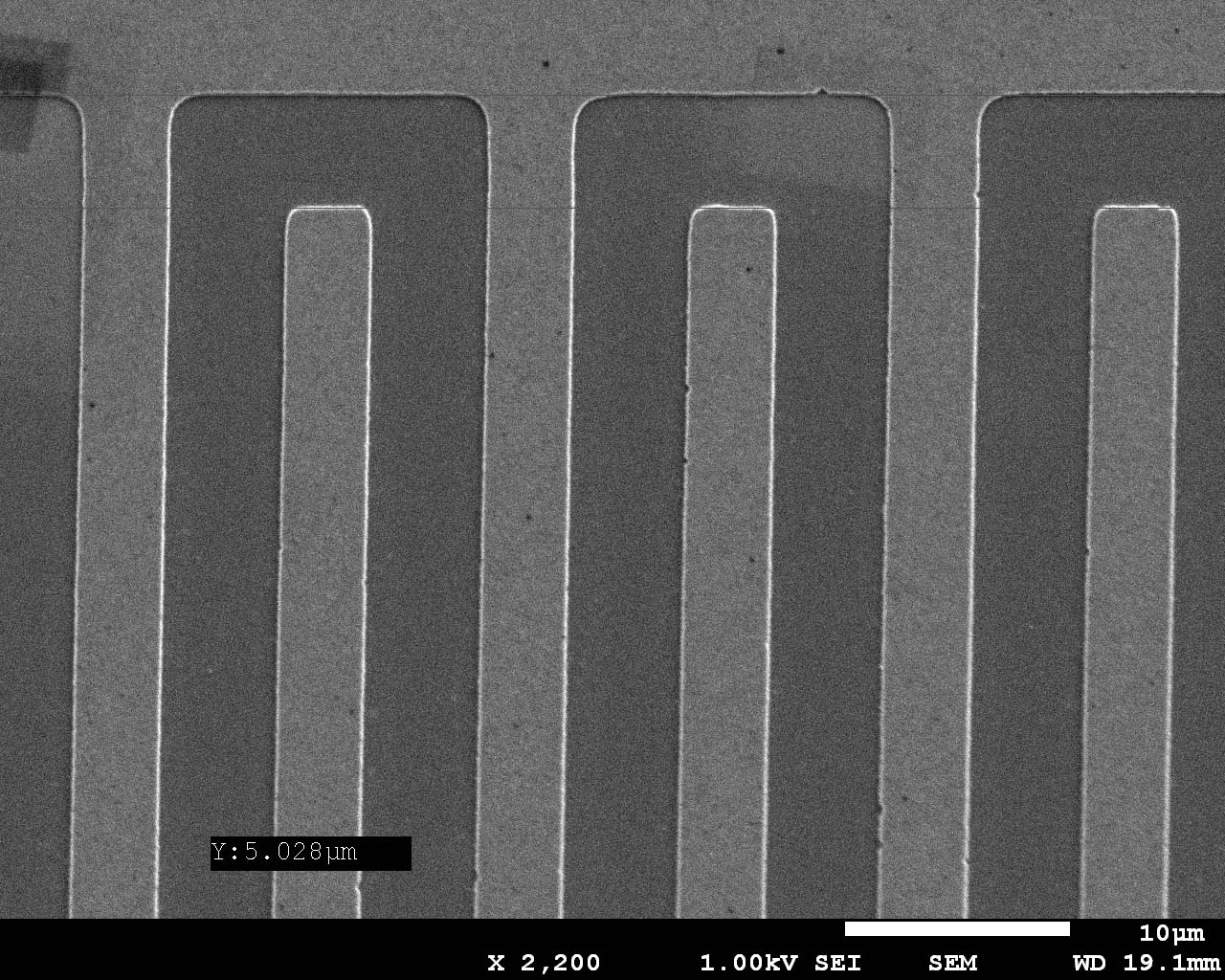
At Microscopy Australia’s University of Queensland facility, the Centre for Microscopy and Microanalysis, scanning electron microscopy was used to monitor edge roughness and optimize device fabrication, while a Dektak profiler was used to calibrate the solutions for the surface treatment. The chips were fabricated at fellow NCRIS facility ANFF. The Atomic Force Microscope was provided by Prof. Rakić’s lab.
Impact
THz SNOM allows for rapid, non-destructive screening of quantum circuitry allowing researchers and businesses to better understand and combat decoherence, and monitor and improve fabrication processes, bringing a viable commercial quantum computer one step closer to reality.
X. Guo et al., Appl. Phys. Lett. 2021 DOI: 10.1063/5.0061078